 |
| click here to join |
SAR study analize reprogram
Wednesday, December 11, 2013
legit new PTC .... the next STAR so bright
Friday, September 6, 2013
Thursday, June 20, 2013
Wednesday, June 19, 2013
Join Now and Start Earning @CnH
Monday, April 9, 2012
Diode
A diode is an electrical device allowing current to move through it in one direction with far greater ease than in the other. The most common kind of diode in modern circuit design is the semiconductor diode, although other diode technologies exist. Semiconductor diodes are symbolized in schematic diagrams such as Figure below. The term “diode” is customarily reserved for small signal devices, I ≤ 1 A. The term rectifier is used for power devices, I > 1 A.

Semiconductor diode schematic symbol: Arrows indicate the direction of electron current flow.
When placed in a simple battery-lamp circuit, the diode will either allow or prevent current through the lamp, depending on the polarity of the applied voltage. (Figure below)

Diode operation: (a) Current flow is permitted; the diode is forward biased. (b) Current flow is prohibited; the diode is reversed biased.
When the polarity of the battery is such that electrons are allowed to flow through the diode, the diode is said to be forward-biased. Conversely, when the battery is “backward” and the diode blocks current, the diode is said to be reverse-biased. A diode may be thought of as like a switch: “closed” when forward-biased and “open” when reverse-biased.
Oddly enough, the direction of the diode symbol's “arrowhead” points against the direction of electron flow. This is because the diode symbol was invented by engineers, who predominantly use conventional flow notation in their schematics, showing current as a flow of charge from the positive (+) side of the voltage source to the negative (-). This convention holds true for all semiconductor symbols possessing “arrowheads:” the arrow points in the permitted direction of conventional flow, and against the permitted direction of electron flow.
Diode behavior is analogous to the behavior of a hydraulic device called a check valve. A check valve allows fluid flow through it in only one direction as in Figure below.
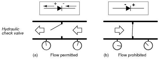
Hydraulic check valve analogy: (a) Electron current flow permitted. (b) Current flow prohibited.
Check valves are essentially pressure-operated devices: they open and allow flow if the pressure across them is of the correct “polarity” to open the gate (in the analogy shown, greater fluid pressure on the right than on the left). If the pressure is of the opposite “polarity,” the pressure difference across the check valve will close and hold the gate so that no flow occurs.
Like check valves, diodes are essentially “pressure-” operated (voltage-operated) devices. The essential difference between forward-bias and reverse-bias is the polarity of the voltage dropped across the diode. Let's take a closer look at the simple battery-diode-lamp circuit shown earlier, this time investigating voltage drops across the various components in Figure below.
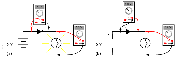
Diode circuit voltage measurements: (a) Forward biased. (b) Reverse biased.
A forward-biased diode conducts current and drops a small voltage across it, leaving most of the battery voltage dropped across the lamp. If the battery's polarity is reversed, the diode becomes reverse-biased, and drops all of the battery's voltage leaving none for the lamp. If we consider the diode to be a self-actuating switch (closed in the forward-bias mode and open in the reverse-bias mode), this behavior makes sense. The most substantial difference is that the diode drops a lot more voltage when conducting than the average mechanical switch (0.7 volts versus tens of millivolts).
This forward-bias voltage drop exhibited by the diode is due to the action of the depletion region formed by the P-N junction under the influence of an applied voltage. If no voltage applied is across a semiconductor diode, a thin depletion region exists around the region of the P-N junction, preventing current flow. (Figure below (a)) The depletion region is almost devoid of available charge carriers, and acts as an insulator:
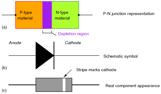
Diode representations: PN-junction model, schematic symbol, physical part.
The schematic symbol of the diode is shown in Figure above (b) such that the anode (pointing end) corresponds to the P-type semiconductor at (a). The cathode bar, non-pointing end, at (b) corresponds to the N-type material at (a). Also note that the cathode stripe on the physical part (c) corresponds to the cathode on the symbol.
If a reverse-biasing voltage is applied across the P-N junction, this depletion region expands, further resisting any current through it. (Figure below)

Depletion region expands with reverse bias.
Conversely, if a forward-biasing voltage is applied across the P-N junction, the depletion region collapses becoming thinner. The diode becomes less resistive to current through it. In order for a sustained current to go through the diode; though, the depletion region must be fully collapsed by the applied voltage. This takes a certain minimum voltage to accomplish, called the forward voltage as illustrated in Figure below.
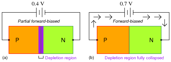
Inceasing forward bias from (a) to (b) decreases depletion region thickness.
For silicon diodes, the typical forward voltage is 0.7 volts, nominal. For germanium diodes, the forward voltage is only 0.3 volts. The chemical constituency of the P-N junction comprising the diode accounts for its nominal forward voltage figure, which is why silicon and germanium diodes have such different forward voltages. Forward voltage drop remains approximately constant for a wide range of diode currents, meaning that diode voltage drop is not like that of a resistor or even a normal (closed) switch. For most simplified circuit analysis, the voltage drop across a conducting diode may be considered constant at the nominal figure and not related to the amount of current.
Actually, forward voltage drop is more complex. An equation describes the exact current through a diode, given the voltage dropped across the junction, the temperature of the junction, and several physical constants. It is commonly known as the diode equation:

The term kT/q describes the voltage produced within the P-N junction due to the action of temperature, and is called the thermal voltage, or Vt of the junction. At room temperature, this is about 26 millivolts. Knowing this, and assuming a “nonideality” coefficient of 1, we may simplify the diode equation and re-write it as such:

You need not be familiar with the “diode equation” to analyze simple diode circuits. Just understand that the voltage dropped across a current-conducting diode does change with the amount of current going through it, but that this change is fairly small over a wide range of currents. This is why many textbooks simply say the voltage drop across a conducting, semiconductor diode remains constant at 0.7 volts for silicon and 0.3 volts for germanium. However, some circuits intentionally make use of the P-N junction's inherent exponential current/voltage relationship and thus can only be understood in the context of this equation. Also, since temperature is a factor in the diode equation, a forward-biased P-N junction may also be used as a temperature-sensing device, and thus can only be understood if one has a conceptual grasp on this mathematical relationship.
A reverse-biased diode prevents current from going through it, due to the expanded depletion region. In actuality, a very small amount of current can and does go through a reverse-biased diode, called the leakage current, but it can be ignored for most purposes. The ability of a diode to withstand reverse-bias voltages is limited, as it is for any insulator. If the applied reverse-bias voltage becomes too great, the diode will experience a condition known as breakdown (Figure below), which is usually destructive. A diode's maximum reverse-bias voltage rating is known as the Peak Inverse Voltage, or PIV, and may be obtained from the manufacturer. Like forward voltage, the PIV rating of a diode varies with temperature, except that PIV increases with increased temperature and decreases as the diode becomes cooler -- exactly opposite that of forward voltage.
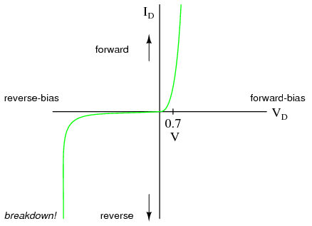
Diode curve: showing knee at 0.7 V forward bias for Si, and reverse breakdown.
Typically, the PIV rating of a generic “rectifier” diode is at least 50 volts at room temperature. Diodes with PIV ratings in the many thousands of volts are available for modest prices.
- REVIEW:
- A diode is an electrical component acting as a one-way valve for current.
- When voltage is applied across a diode in such a way that the diode allows current, the diode is said to be forward-biased.
- When voltage is applied across a diode in such a way that the diode prohibits current, the diode is said to be reverse-biased.
- The voltage dropped across a conducting, forward-biased diode is called the forward voltage. Forward voltage for a diode varies only slightly for changes in forward current and temperature, and is fixed by the chemical composition of the P-N junction.
- Silicon diodes have a forward voltage of approximately 0.7 volts.
- Germanium diodes have a forward voltage of approximately 0.3 volts.
- The maximum reverse-bias voltage that a diode can withstand without “breaking down” is called the Peak Inverse Voltage, or PIV rating.
Saturday, April 7, 2012
TRANSISTOR

History :
A transistor is a sandwich of dissimilar semiconductors to which are attached three electrodes. …
(credit: © Merriam-Webster Inc.)
Solid-state semiconductor device for amplifying, controlling, and generating electrical signals. Invented at Bell Labs (1947) by John Bardeen, Walter H. Brattain, and William B. Shockley, it displaced the vacuum tube in many applications. Transistors consist of layers of different semiconductors produced by addition of impurities (such as arsenic or boron) to silicon. These impurities affect the way electric current moves through the silicon. Transistors were pivotal in the advancement of electronics because of their small size, low power requirements, low heat generation, modest cost, reliability, and speed of operation. Single transistors were superseded in the 1960s and '70s by integrated circuits; present-day computer chips contain millions of transistors. Today transistors perform many different functions in nearly every type of electronic equipment.
A transistor is a semiconductor designed to operate as an amplifier or a switch. A transistor has three parts: a base (B), a collector (C), and an emitter (E).

When a certain amount of current passes through the base, the current flowing from the collector to the emitter can be regulated. When used as an amplifier, a small current flowing through B can cause the larger current flowing through C to pass through the gate to E. When used as a switch, the base voltage must rise above a certain amount (for example, 5 volts) before the current flows to E. Transistors are a fundamental part of today's electronic devices, including radios, televisions, and computers. A modern computer has hundreds of millions of transistors.
The Basic usage :
In the analog world of continuously varying signals, a transistor is a device used to amplify its electrical input. In the digital world of computing, a transistor is mostly a binary switch and the fundamental building block of digital circuitry. Like a light switch on the wall, the transistor acts as a simple on/off switch, either preventing or allowing current to flow through.
Common Types :
The transistor is an arrangement of semiconductor
materials that share common physical boundaries. Materials most commonly used are silicon, gallium-arsenide, and germanium, into which impurities have been introduced by a process called "doping." In n-type semiconductors the impurities or dopants result in an excess of electrons, or negative charges; in p-type semiconductors the dopants lead to a deficiency of electrons and therefore an excess of positive charge carriers or "holes."
The Junction Transistor
The n-p-n junction transistor consists of two n-type semiconductors (called the emitter and collector) separated by a thin layer of p-type semiconductor (called the base). The transistor action is such that if the electric potentials on the segments are properly determined, a small current between the base and emitter connections results in a large current between the emitter and collector connections, thus producing current amplification. Some circuits are designed to use the transistor as a switching device; current in the base-emitter junction creates a low-resistance path between the collector and emitter. The p-n-p junction transistor, consisting of a thin layer of n-type semiconductor lying between two p-type semiconductors, works in the same manner, except that all polarities are reversed.
The Field-Effect Transistor
A very important type of transistor developed after the junction transistor is the field-effect transistor (FET). It draws virtually no power from an input signal, overcoming a major disadvantage of the junction transistor. An n-channel FET consists of a bar (channel) of n-type semiconductor material that passes between and makes contact with two small regions of p-type material near its center. The terminals attached to the ends of the channel are called the source and the drain; those attached to the two p-type regions are called gates. A voltage applied to the gates is directed so that no current exists across the junctions between the p- and n-type materials; for this reason it is called a reverse voltage. Variations of the magnitude of the reverse voltage cause variations in the resistance of the channel, enabling the reverse voltage to control the current in the channel. A p-channel device works the same way but with all polarities reversed.
The metal-oxide semiconductor field-effect transistor (MOSFET) is a variant in which a single gate is separated from the channel by a layer of metal oxide, which acts as an insulator, or dielectric. The electric field of the gate extends through the dielectric and controls the resistance of the channel. In this device the input signal, which is applied to the gate, can increase the current through the channel as well as decrease it.


